RK3399 VOP Performance and Bandwidth Analysis Report
ID: RK-KF-YF-125
Release Version: V1.0.0
Date: 2020-8-18
Security Level: □Top-Secret □Secret ■Internal □Public
DISCLAIMER
This document is provided "as is". Rockchip Electronics Co., Ltd. ("the Company") makes no express or implied representations or warranties regarding the accuracy, reliability, completeness, merchantability, fitness for a particular purpose, or non-infringement of any statements, information, or content in this document. This document is for reference as a usage guide only.
Due to product version upgrades or other reasons, this document may be updated or modified from time to time without any notice.
Trademark Statement
"Rockchip", "Rockchip", and "Rockchip" are registered trademarks of the Company and belong to the Company.
All other registered trademarks or trademarks mentioned in this document are owned by their respective owners.
Copyright © 2020 Rockchip Electronics Co., Ltd.
Beyond the scope of fair use, without the written permission of the Company, no individual or entity may excerpt, copy, or distribute any part or all of the content of this document in any form.
Rockchip Electronics Co., Ltd.
Address: No. 18, Area A, Software Park, Tongpan Road, Fuzhou, Fujian Province
Website: www.rock-chips.com
Customer Service Tel: +86-4007-700-590
Customer Service Fax: +86-591-83951833
Customer Service Email: fae@rock-chips.com
Preface
Overview
Intended Audience
This document (guide) is mainly applicable to the following engineers:
Rockchip Graphics/Display Module Development Engineers
Revision History
| Version | Author | Date | Description |
|---|---|---|---|
| V1.0.0 | Huang Jiachai | 2020-08-27 | Initial version |
[TOC]
Experiment Purpose
To address frequent display flickering and insufficient bandwidth issues on Rockchip platforms, analyze VOP bus access behavior based on different VOP scene configurations combined with oscilloscope measurement of DDR DQS signals. The goal is to find the causes and bottlenecks of current problems and provide solutions for future IP design.
Experiment Personnel
General Engineering Office: Zhang Chongsong
Platform Center: He Canyang, Huang Jiachai
Test Environment
Hardware Environment
Oscilloscope: Agilent Technologies MSO9254A 2.5 GHz, Probe: 1131A 3.5GHz
EVB Board: RK_IND_EVB_RK3399_LP4D200P232SD8_V12_20200109YWQ
DDR Type: LPDDR4
Software Environment
Software Version: Android 10.0, Linux 4.19 kernel
Firmware Backup: [RK3399 Android 10.0 IND](\10.10.10.164\Q_Repository\RK3399\MID\firmware\rk3399-evb-ind\RK3399 VOP Performance And Bandwidth Analysis)
Android Property Configuration:
| Property | Function |
|---|---|
| vendor.hwc.device.main=HDMI-A | Set HDMI as primary display |
| vendor.hwc.compose_policy=0 | Disable hwc, ensure only one layer |
| persist.vendor.framebuffer.main=3840x2160@60 | Set 4k UI |
| vendor.gralloc.disable_afbc=1 | Disable AFBC by default |
Test Points
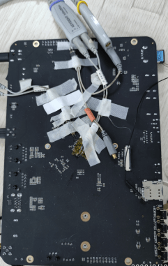
DDR channel 0 DQS --> Oscilloscope blue line:
DDR channel 1 DQS --> Oscilloscope green line:
VOP DEN --> Oscilloscope yellow line:
Related Concepts
Using RK3399 LPDDR4 platform as an example:
- VOP burst: The bus bandwidth is 128 bit, so one aclk cycle accesses 128 bit data. The VOP default configuration is burst 16, so one burst 16 is 128 bit x 16 / 8bit = 256 Byte;
- VOP gather: When gather is enabled, VOP issues as many consecutive burst accesses as possible. For example, gather8, without considering bus bandwidth and VOP processing performance, VOP issues 256 Byte x 8 = 2048 Byte of access requests at a time;
- VOP max outstanding: The number of DMA requests continuously issued by VOP, i.e., the maximum number of access requests that can be issued before the previous DMA request returns;
- DDR burst: Each DDR clk accesses 32 bit x 2(DDR) / 8 bit = 8 Byte. LPDDR4 defaults to burst 16, so one DDR burst8 is 8 x 8 = 128 Byte;
- DDR stride: The interleaving granularity between two DDR channels, default is 256 Byte (i.e., switching DDR channels every 256 Byte), can also be configured to 512 Byte, 4096 Byte, etc.
Experiment Process
Experiment 1: VOP Gather Effect Verification
Related Configuration
- DDR Frequency: 856 MHz
- VOP ACLK: 400 MHz
- Output Resolution: 3840x2160@60
Signal Diagrams Under Different Configurations
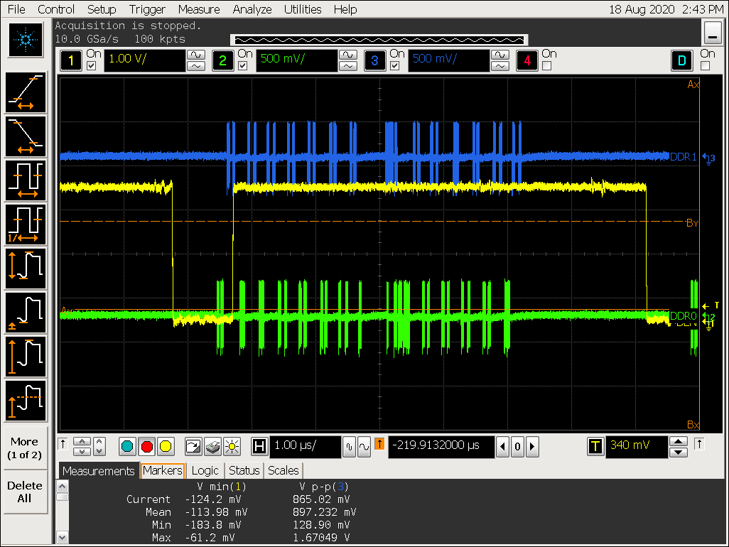
3840x2160@ARGB
-
Gather disabled signal
-
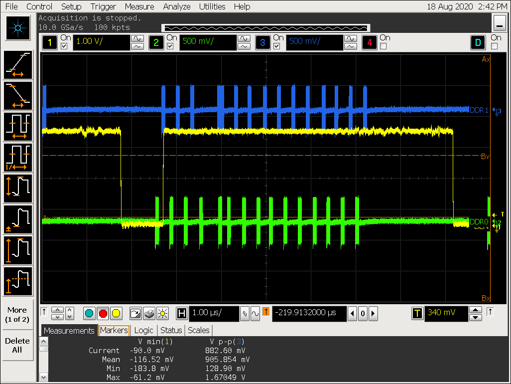
Gather enabled with win0_yrgb_axi_gather_num = 1, i.e., gather 2
-
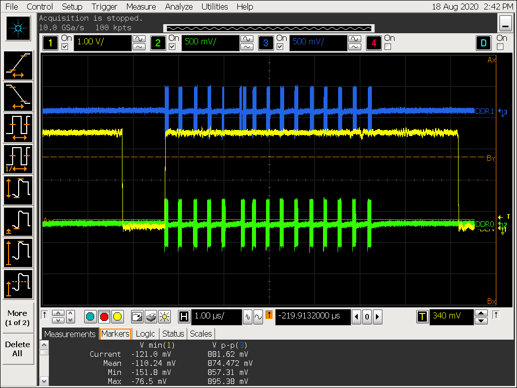
Gather enabled with win0_yrgb_axi_gather_num = 2, i.e., gather 4
-
Gather enabled with win0_yrgb_axi_gather_num = 3, i.e., gather 8
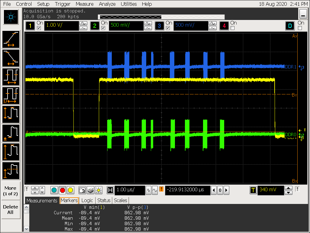
-
Gather enabled with win0_yrgb_axi_gather_num = 4, i.e., gather 16
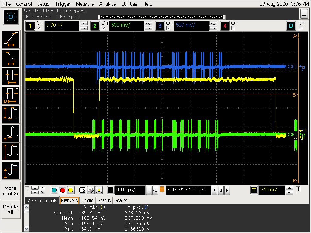
3840x2160@YUV420SP_10bit
To ensure the Android display framework can overlay 4k yuv data to VOP for display, enable hwc module and configure the property:
setprop vendor.hwc.compose_policy 6
-
Gather disabled signal
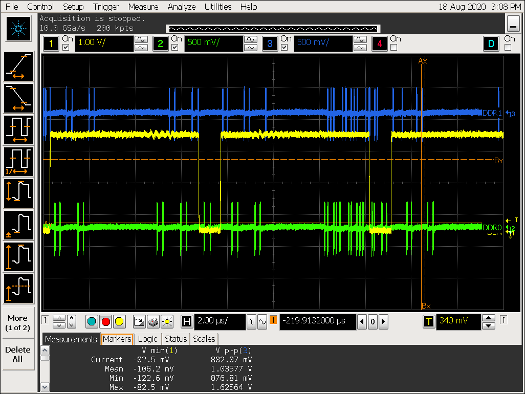
-
Gather enabled with win0_yrgb_axi_gather_num = 1, win0_cbr_axi_gather_num = 1, i.e., gather 2
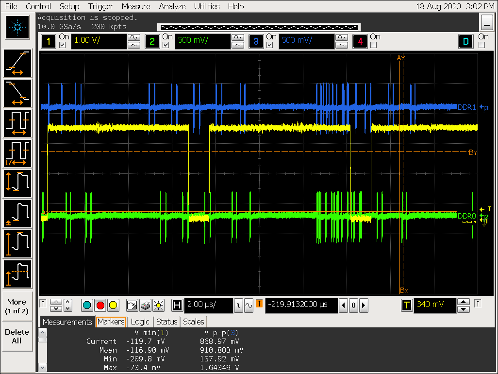
-
Gather enabled with win0_yrgb_axi_gather_num = 2, win0_cbr_axi_gather_num = 2, i.e., gather 4
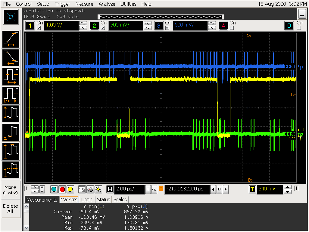
-
Gather enabled with win0_yrgb_axi_gather_num = 3, win0_cbr_axi_gather_num = 3, i.e., gather 8
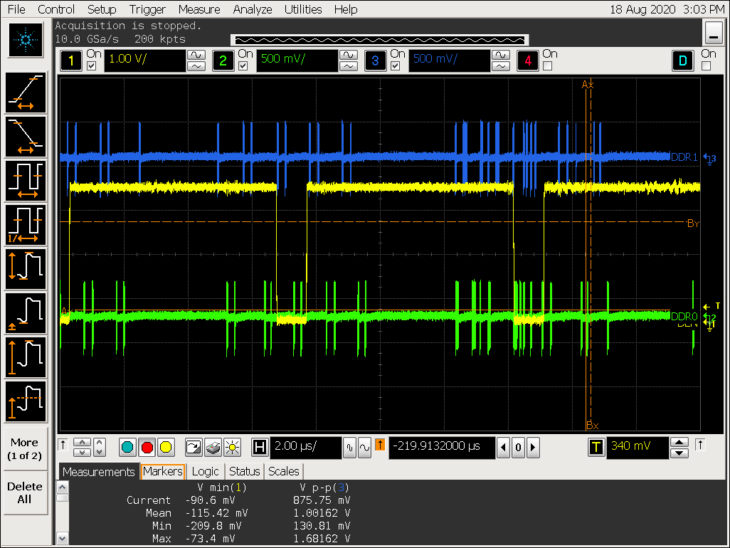
-
Gather enabled with win0_yrgb_axi_gather_num = 4, win0_cbr_axi_gather_num = 4, i.e., gather 16
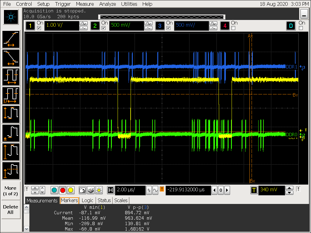
Experiment 1 Conclusion
- ARGB8888 format supports up to gather 8. After enabling gather, DDR access is noticeably more concentrated, but VOP configurations exceeding gather 8 will cause the gather effect to be disabled;
- For YUV420SP, enabling or disabling gather makes little difference;
Experiment 2: Max Outstanding Verification
Purpose
Analyze the VOP outstanding size in combination with DDR stride and VOP gather configurations;
Related Configuration
- DDR Frequency: 856 MHz, default stride: 256 Byte
- VOP ACLK: 400 MHz, bus width: 128 bit
- Output Resolution: 3840x2160@60
- VOP win3 enabled, data size and format: 3840x2160@ARGB8888
- VOP burst 16, gather 8 enabled, max outstanding 30
Signal Diagrams
VOP scan line access behavior
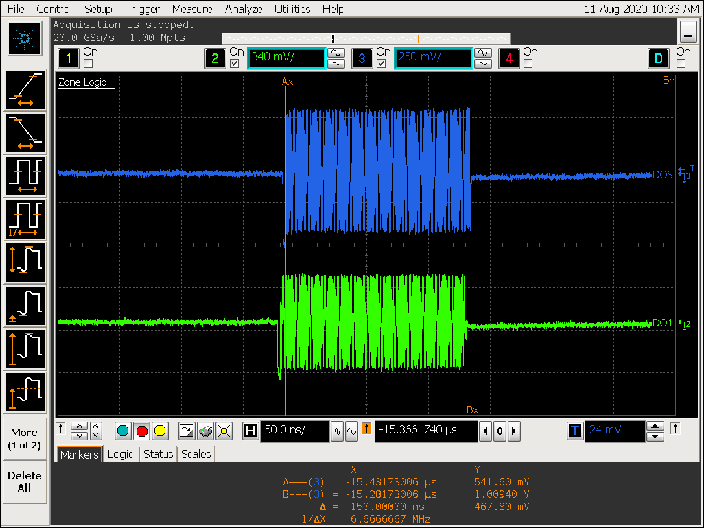
DDR channel 0 DQS consecutive burst access
Data Analysis
- Theoretical data volume
DDR bandwidth: 856 MHz x 32 bit x 2(DDR) x 2 channel / 8 bit = 13,696 MBps
VOP AXI bus bandwidth: 128 bit x 400 MHz / 8bit = 6400 MBps
VOP gather 8 data volume: 128 bit x 16 (burst 16) x 8 (gather 8) / 8 bit = 2048 Byte
VOP scan line data volume: 3840 pixel x 4 Byte = 15,360 Byte
- Measured data volume
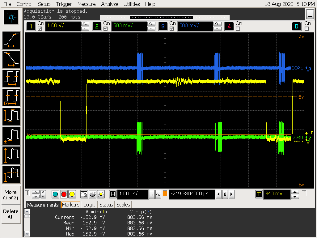
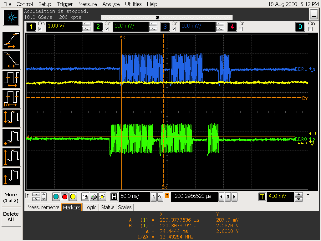
From the images above, the DDR consecutive burst time is: 150 ns, i.e., 150ns / (1000 / 856) = 128 cycles, corresponding data volume: 128 x 32 x 2(DDR) x 2 channel / 8 bit = 2048 Byte;
VOP one burst data volume: 128 bit x 16 (burst 16) / 8 bit = 256 Byte
(DDR consecutive burst data volume) / (VOP one burst data volume) = 2048 Byte / 256 Byte = 8, consistent with the gather 8 configuration expectation;
Signal after lowering VOP ACLK
-
VOP ACLK default 400M
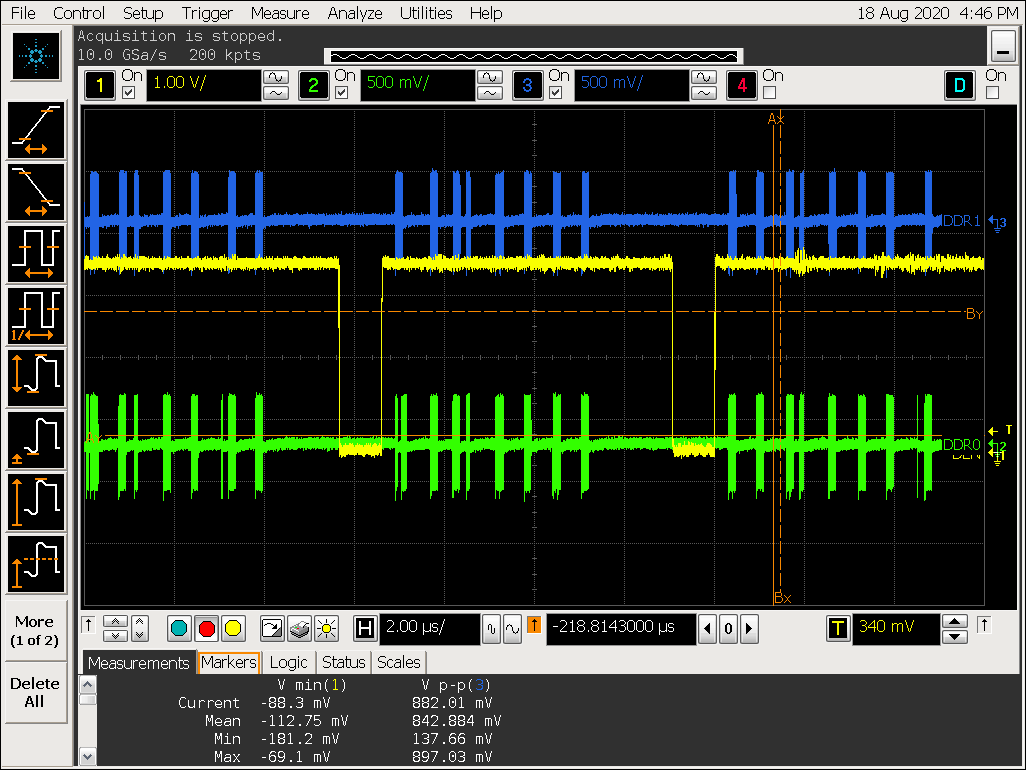
-
VOP ACLK lowered to 300M
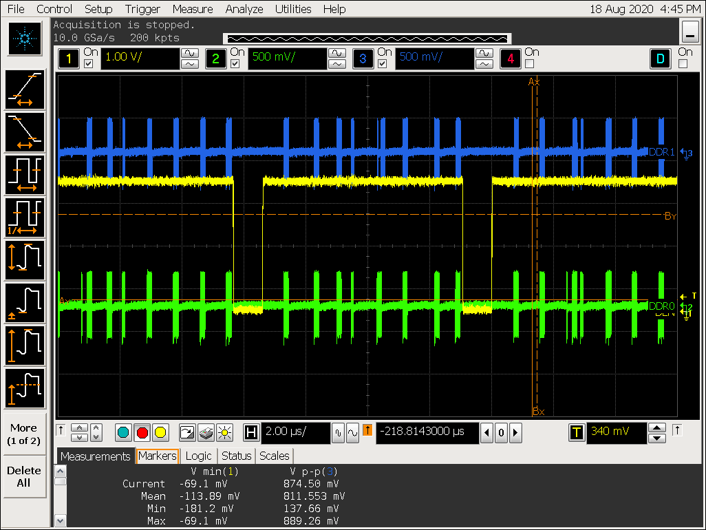
-
VOP ACLK lowered to 200M
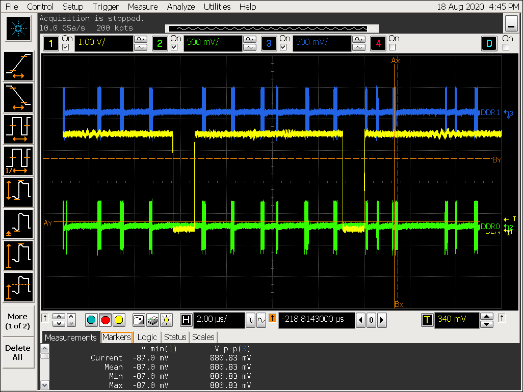
First consecutive burst access diagram enlarged:
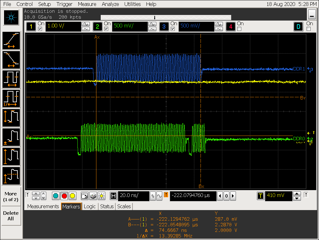
-
VOP ACLK lowered to 100M
First consecutive burst access diagram enlarged:
Experiment 2 Conclusion
- From the above images, as ACLK decreases, the VOP data fetch time increases;
- Theoretically, VOP ACLK 200M can provide data bandwidth of: 200M x 128 bit / 8 = 3200M, VOP 4k ARGB data requires 1898M, so theoretically 200M aclk is sufficient, but actual testing shows abnormal flickering and insufficient bandwidth at ACLK 200M;
- After reducing VOP ACLK to 200M, DDR consecutive burst decreased from 128 cycles to 64 cycles;
- Further confirmation with IC team: data fetched by VOP from the AXI bus must go through internal processing logic before being placed in the linebuffer. Limited by VOP internal processing speed, VOP cannot receive all the data the bus provides;
Next Generation VOP Design
- RK3566 VOP Cluster layers have a front-end linebuffer added, allowing data to be filled into the linebuffer quickly and centrally, without VOP internal processing efficiency limitations. This also requires only one request per line. However, smart and esmart layers maintain the RK3399 design;
- Discussion with IC team: for RK3588, front-end linebuffers will also be added to smart and esmart layers to ensure data can be fetched from the bus to the linebuffer quickly at once, which not only provides friendlier DDR access behavior but also improves VOP bandwidth issues;
Experiment 3: DEN and DQS Phase
Phase of VOP DEN Signal and DDR DQS Signal
- VOP gather disabled
- VOP gather enabled
Experiment 3 Conclusion
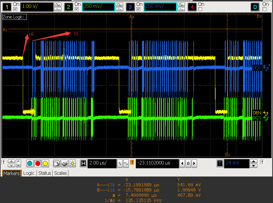
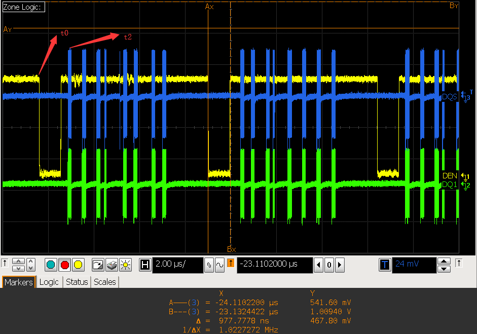
From the two images above, at the point where den ends (i.e., when the VOP has finished sending the previous line of data), at this moment the VOP linebuffer is empty, but VOP does not immediately start fetching data; instead it waits for some time:
- When gather is disabled, the waiting time is approximately: T = t1-t0 ≈ 0.8us, accounting for 10.8% of the total 7.4us per line;
- When gather is enabled, the waiting time is approximately: T = t2-t0 ≈ 1.2us, accounting for 16.2% of the total 7.4us per line;
- During this time, VOP does not fetch data in time, wasting the opportunity for early data fetching. It is recommended that IC advance the data fetch timing to the position where den ends;
- At the same time, IC needs to investigate why enabling or disabling gather causes T to be inconsistent;
Experiment 4: DDR Stride Effect Verification
DDR Stride Experiment Process
-
Change DDR stride from 256 Byte to 4K Byte;
-
Set CPU to performance mode, fixed frequency 1416000 Hz;
echo performance > /sys/devices/system/cpu/cpufreq/policy0/scaling_governorcat /sys/devices/system/cpu/cpufreq/policy0/cpuinfo_cur_freq1416000 -
VOP ACLK default configuration 600M waveform:
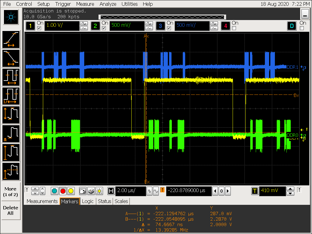
- Execute micro_bench_arm32 to test CPU memset speed: 4960MB/s
- Change ACLK from 600M to 100M, waveform:
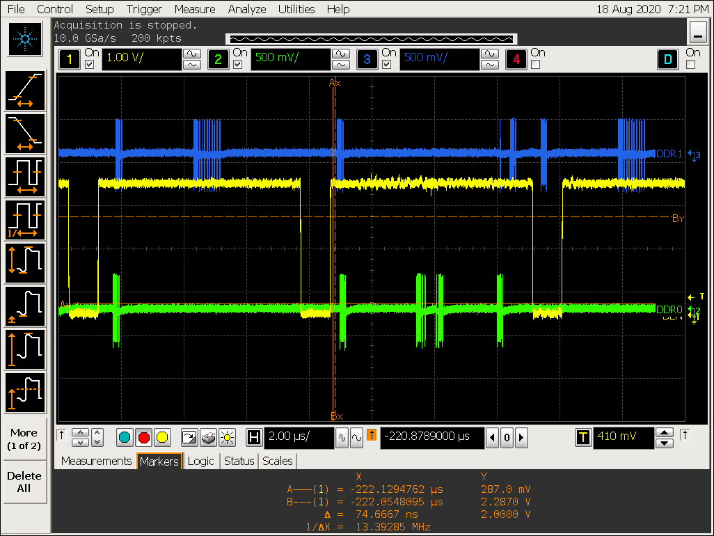
- Execute micro_bench_arm32 to test CPU memset speed: 5200MB/s
- Move mouse to observe if any GPU access behavior is inserted
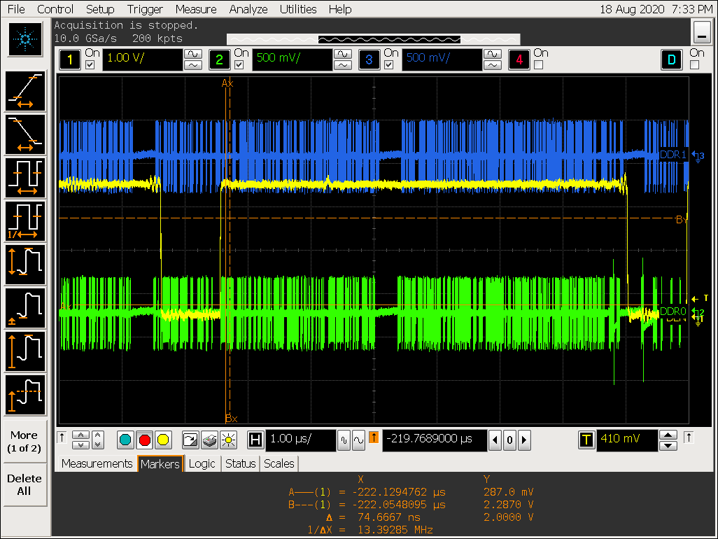
Experiment 4 Conclusion
When VOP data fetching is insufficient, the bus is not held, meaning other IPs can insert accesses;
Experiment 5: AFBC Format Access Behavior
Related Configuration
- DDR stride 4K Byte;
- VOP aclk 400M;
- Enable VOP afbc function;
setprop vendor.gralloc.disable_afbc 0
- Since RK3399 VOP AFBC supports a maximum input of 2560, set the Android framebuffer size to 1080p, and switch HDMI output resolution to 1080p 60hz;
setprop persist.vendor.framebuffer.main 1920x1080p60
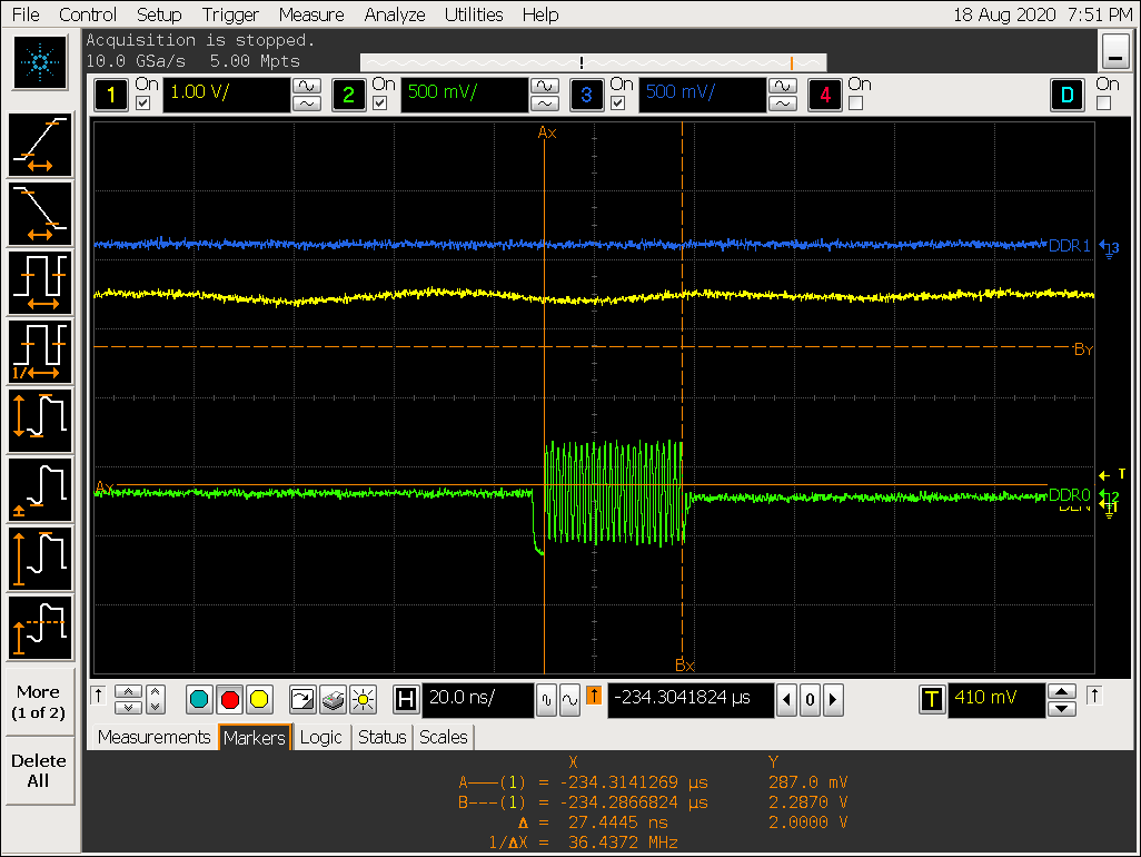
UI Scene Test
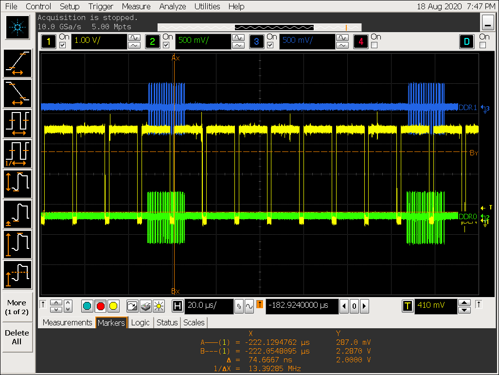
Enlarged view 1:
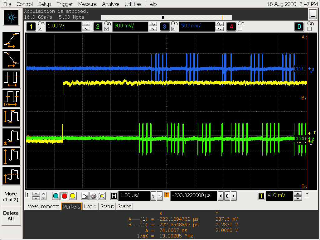
Enlarged view 2:
Video Scene Test
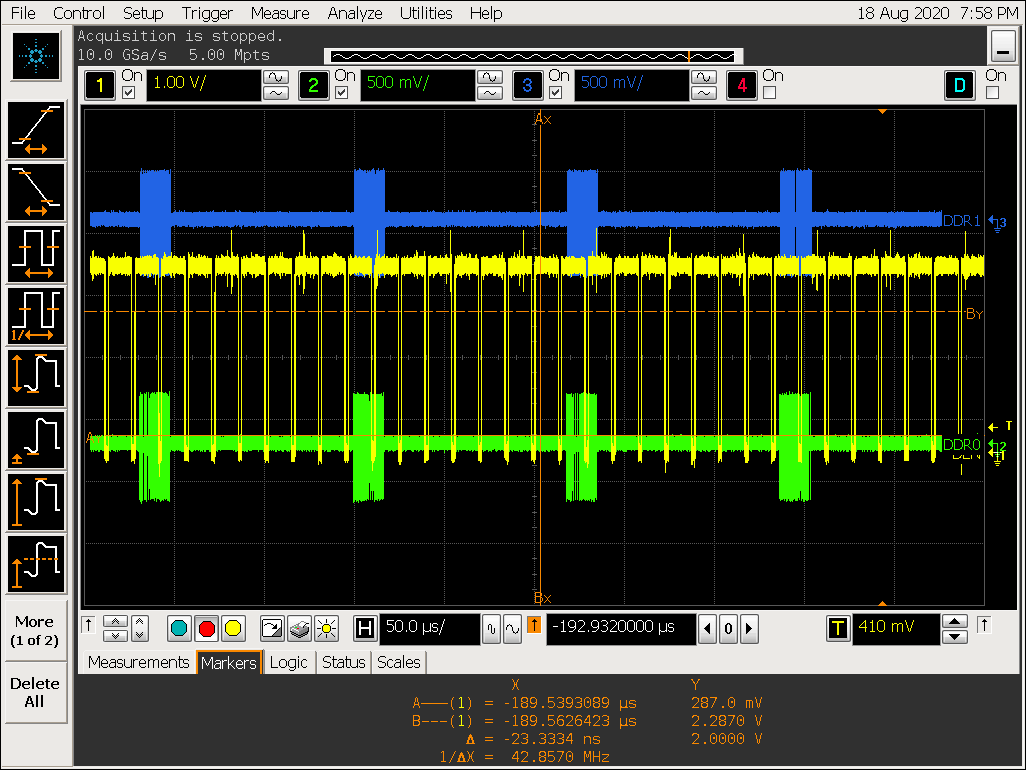
Enlarged view 1:
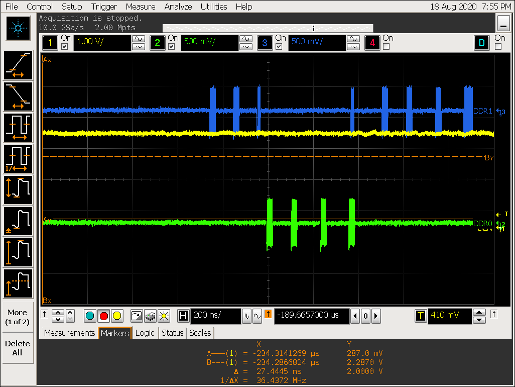
Enlarged view 2:
Experiment 5 Conclusion
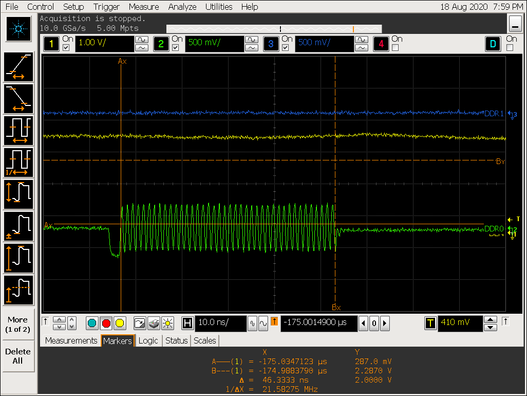
- RK3399 AFBC tile size: 16x8 pixels. From the waveforms, concentrated data fetching occurs every 8 lines;
- Data format is ARGB8888. GPU encodes as 16 x 16 x 4 = 1024 Byte per tile, so the address jump between tiles is 1024 Byte. DDR stride is 4K Byte, so DDR interleaves every 4 tiles [switches DDR channel];
- In UI scene, randomly captured tile data volume: 27.4ns / (1000 / 856) x 32 x 2 / 8 = 192 Byte, i.e., current tile compression ratio: 192 / 512 = 37.5%;
- In video scene, randomly captured tile data volume: 46.3ns / (1000 / 856) x 32 x 2 / 8 = 318 Byte, i.e., current tile compression ratio: 318 / 512 = 62%;
- Each tile has a 128-bit header and a payload stored at different addresses. Currently, the RK3399 design fetches: 4 tile headers -> 4 payloads -> 4 tile headers -> 4 payloads... The data volume of 4 headers is only 512 bits, which is inefficient;
Experiment Summary
- The main cause of flickering during 4k video/4k UI playback on RK3399 platform is that the VOP processing unit operates in the ACLK domain, and the ACLK design at 400M cannot meet the requirements of this scenario;
- VOP does not fetch data in time when the linebuffer is idle, wasting effective data fetch time. It is recommended that IC advance the data fetch behavior in future designs;
- Under different VOP gather configurations, the timing of data fetching start and the phase of VOP DEN are not fixed, requiring further investigation by IC;
- It is recommended that all layers in future VOP designs include front-end linebuffers to ensure data can be fetched from the bus to the linebuffer quickly at once, which not only provides friendlier DDR access behavior but also prevents VOP data fetching from being affected by VOP internal processing speed;
- Changing AFBC data to fetch one line of headers continuously can improve DDR access efficiency;