Overview
The RF-OV5695-JD01 V1.0 camera module uses the OmniVision OV5695 color CMOS image sensor and provides 5-megapixel image output.
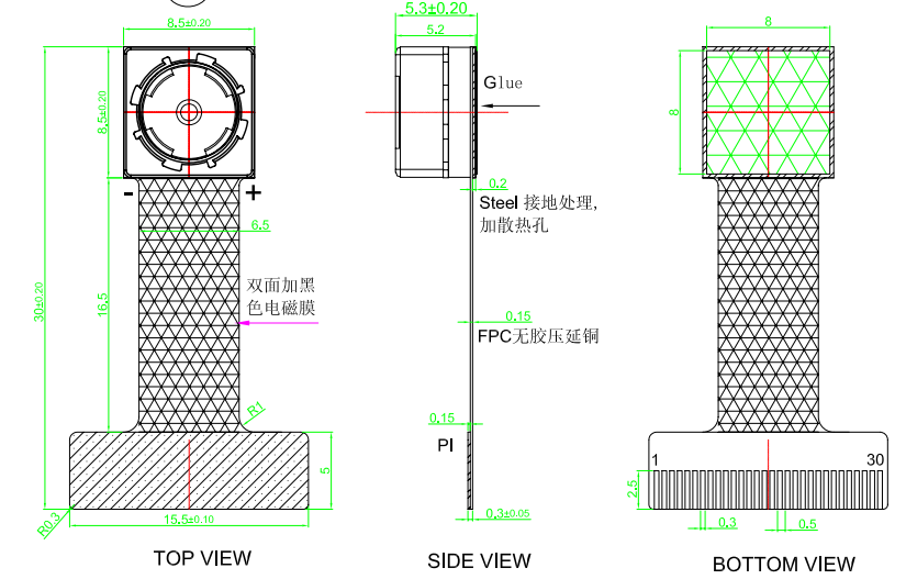
The module drawing shows a 30-pin FPC connector. Two MIPI data lanes are connected, together with the MIPI clock pair, I2C, MCLK, PWDN, and three sensor power rails.
Main Specifications
| Item | Specification |
|---|
| Module model | RF-OV5695-JD01 V1.0 |
| Image sensor | OmniVision OV5695 |
| Sensor type | Color CMOS, rolling shutter |
| Active resolution | 2592 × 1944 |
| Resolution | Approximately 5 megapixels |
| Optical format | 1/4 inch |
| Pixel size | 1.4 μm × 1.4 μm |
| Pixel technology | OmniBSI+ |
| Output format | 10-bit RGB RAW |
| Data interface | MIPI |
| MIPI lanes | One or two lanes supported; this module connects two lanes |
| Control interface | SCCB / I2C |
| HDR | Interleave Row HDR |
| Image functions | Mirror, flip, crop, windowing, and 2 × binning |
| OTP | 16 bytes available to users |
| Drawing output note | RGB Output |
Resolution and Frame Rate
| Output Mode | Resolution | Maximum Frame Rate |
|---|
| Full resolution | 2592 × 1944 | 30 fps |
| Quad HD | 2560 × 1440 | Depends on register configuration |
| Full HD | 1920 × 1080 | Depends on register configuration |
| HD | 1280 × 720 | Depends on register configuration |
| VGA | 640 × 480 | Depends on register configuration |
Lens Parameters
| Item | Specification |
|---|
| Focusing range | 10 cm to infinity |
| Focal length | 3.75 mm |
| Aperture | F2.8 |
| Diagonal field of view | 70° |
| TV distortion | Less than 1% |
Electrical Parameters
| Supply or Signal | Specification |
|---|
| AVDD | 2.8 V; sensor range 2.7 V to 3.0 V |
| DVDD | 1.2 V; sensor range 1.14 V to 1.26 V |
| DOVDD | 1.8 V; sensor range 1.7 V to 1.9 V |
| AF-VDD | 2.8 V |
| MCLK | External sensor master clock |
| PWDN | Hardware power-down control |
| RESET | Marked NC in the drawing; verify against the module schematic |
| SCL / SDA | I2C control bus |
30-Pin Connector
| Pin | Signal | Description |
|---|
| 1 | GND | Ground |
| 2 | MCP | MIPI clock positive |
| 3 | MCN | MIPI clock negative |
| 4 | GND | Ground |
| 5 | MDP0 | MIPI data lane 0 positive |
| 6 | MDN0 | MIPI data lane 0 negative |
| 7 | GND | Ground |
| 8 | MDP1 | MIPI data lane 1 positive |
| 9 | MDN1 | MIPI data lane 1 negative |
| 10 | GND | Ground |
| 11 | MDP2 (NC) | Not connected |
| 12 | MDN2 (NC) | Not connected |
| 13 | GND | Ground |
| 14 | MDP3 (NC) | Not connected |
| 15 | MDN3 (NC) | Not connected |
| 16 | GND | Ground |
| 17 | NC | Not connected |
| 18 | NC | Not connected |
| 19 | AF-VDD 2.8 V | Autofocus actuator supply |
| 20 | SCL | I2C clock |
| 21 | SDA | I2C data |
| 22 | MCLK | Sensor master clock |
| 23 | NC | Not connected |
| 24 | PWDN | Power-down control |
| 25 | NC | Not connected |
| 26 | RESET (NC) | Marked not connected |
| 27 | NC | Not connected |
| 28 | DOVDD 1.8 V | I/O supply |
| 29 | AVDD 2.8 V | Analog supply |
| 30 | DVDD 1.2 V | Core supply |
Mechanical Parameters
| Item | Specification |
|---|
| FPC pin count | 30 pins |
| FPC pin pitch | 0.3 mm |
| Reinforcement width | 15.5 ± 0.10 mm |
| Reinforcement height | 5 mm |
| Overall module length | 30 ± 0.20 mm |
| Lens-holder dimensions | 8.5 ± 0.20 mm × 8.5 ± 0.20 mm |
| Side-view height | 5.3 ± 0.20 mm; body marked 5.2 mm |
| Main FPC width | 6.5 mm |
| Effective FPC length | 16.5 mm |
| Rear adhesive area | 8 mm × 8 mm |
| Steel thickness | 0.2 mm |
| PI thickness | 0.15 mm |
| Reinforced tail thickness | 0.3 ± 0.05 mm |
Mechanical and Connector Drawing